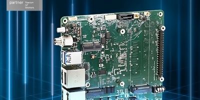
20A models added to 1/16th brick footprint DC-DC buck converter series from TDK

TDK has announced an expansion to the TDK-Lambda i7A series of non-isolated buck (step-down) DC-DC converters with the industry-standard 1/16th brick pinout. 20A output models with a 500W maximum rating are now available, offering a trimmable 3.3 – 32V* output capability and operation from 28V up to 60V input. An adjustable over-current limit is also available as an option, reducing stress on the converter or load when exposed to excessive overcurrent conditions and facilitating fine-tuning based on actual system requirements.

The 20A i7A models can be used to derive additional high-power outputs at a lower cost and higher efficiency than isolated DC-DC converters. These very compact products are suited for use in mobile robotics, drones, medical, industrial, test and measurement, communications, computing, and portable battery-powered equipment.

Efficiencies of up to 96% dramatically minimise internal losses and allow the 20A i7A models to operate in ambient temperatures of -40°C up to +125°C, even with low airflow conditions. The i7A’s design provides low output ripple and excellent response to dynamic loads. Minimal external components are required, compared to discrete solutions, saving cost and printed circuit board space.

Like the i7A 33A, 45A and 60A versions, the 20A offers a choice of three mechanical configurations, measuring just 34mm wide and 36.8mm in length. The 11.5mm high open-frame model is suitable for applications requiring a low profile and weighs just 25g. The baseplate version can be conduction-cooled to a cold plate and is 12.7mm high. Models with an integral heatsink, which are for convection or forced air cooling, are 24.9mm high.

The i7A standard features include output voltage adjustment, positive remote sense, negative logic remote on-off, input under-voltage, over-current and over-temperature protection. Evaluation boards are available for simplified qualification.

All models have safety certification to the IEC/UL/CSA/EN 62368-1 standards, with CE and UKCA marking to the Low Voltage and RoHS Directives.

https://product.tdk.com

> Read More

ROHM develops the industry’s smallest CMOS Op Amp for smartphones and IoT devices

ROHM has developed an ultra-compact 1.8V – 5V, rail-to-rail CMOS operational amplifier (op amp) – the TLR377GYZ. It is optimised for amplifying signals from sensors such as temperature, pressure, flow rate, used in smartphones, small IoT devices, and similar applications.

The size of smartphones and IoT devices continues to decrease – requiring smaller components. To accurately amplify small signals as needed in high precision sensing, op amps must improve low input offset voltage and noise performance while continuing to shrink the form factor.

The TLR377GYZ succeeds in balancing miniaturisation with high accuracy (which has been difficult to achieve with conventional op amps) by further evolving proprietary circuit design, process, and packaging technologies cultivated over many years.

Op amps’ input offset voltage and noise generation degrade amplification accuracy and can be suppressed by increasing the size of the built-in transistors – but at the expense of miniaturisation. In response, ROHM developed proprietary circuits which achieve a maximum offset voltage as low as 1mV without increasing the size of the transistors. In addition, proprietary process technology greatly reduces flicker noise, while ultra-low noise is achieved with an input equivalent noise voltage density of 12nV/√Hz by optimising the resistive components at the element level. Furthermore, the new product adopts a WLCSP (Wafer Level Chip Scale Package) with a ball pitch of just 0.3mm utilising original packaging technology. This reduces size by approximately 69% compared to conventional products and 46% over existing compact products.

https://www.rohm.com/

> Read More

Sondrel’s SFA 100 is ideal for AI at the Edge

Sondrel has optimised its SFA 100 to make it ideal for battery-powered, AI at the Edge applications. The SFA 100 is one of the five architectural platforms in the company’s Architecting the Future chip design platform which provides a ready-made design baseline that the company uses to build a bespoke solution for every customer.

The SFA 100 uses an Arm subsystem with a choice of Arm cores and the option of a security subsystem. Its low power requirement makes it the ideal platform for battery-powered edge AI applications such as smart home, smart factory, and sensor fusion devices. The device provides the ability to integrate a machine-learning engine supporting a variety of inference based ‘smarts’ such as voice activation, image classification, gesture recognition, filtering, etc. A radio subsystem such as a Bluetooth IP block or WiFi can also be added if required. Customer’s IP and any third-party IP can be included as Sondrel has the ability to wrap IP blocks so that they have all the necessary interfaces to just drop onto the chassis. More powerful solutions can be created by using the SFA 200 or SFA 300 as starting points.

The Edge AI market is predicted to expand at a CAGR of 33.5% to reach $76 billion by 2031 according to a report by Transparency Market Research. The key is the drive to process data locally and thus eliminate the latency from transmitting the data to a centralised cloud server for processing. Applications range from industry 4.0, where it is used to provide real-time decision making, to devices such as drones, smartphones, cars, etc.

https://www.sondrel.com/

> Read More

Microchip introduces a new core in the dsPIC digital signal controller family

Microchip has launched its dsPIC33A Core family of Digital Signal Controllers (DSCs). The ability for engineers to create sophisticated, computationally intensive embedded control algorithms is crucial for achieving superior operational efficiency in motor control, power supply, charging and sensing systems. Built around a 32-bit Central Processing Unit (CPU) architecture with a 200 MHz operating speed, the dsPIC33A family’s advanced core includes a Double-Precision Floating-Point Unit (DP FPU) and DSP instructions for numerically intensive tasks in many closed-loop control algorithms. The dsPIC33A architecture offers high-performance and precise real-time control coupled with a comprehensive development tool ecosystem to streamline and accelerate the design process.

The dsPIC33A DSCs are enhanced with improved maths and data processing, higher code efficiency, faster context switching and reduced latency. This lower latency allows for a faster response time to transient and safety-critical events. New and upgraded peripherals—such as high-resolution PWMs specifically engineered for motor control and digital power conversion—are designed to support progressive technology development in various markets including automotive, industrial, consumer, E-Mobility, data centre and sustainable solutions segments. The dsPIC33A family features integrated analog peripherals, including 12-bit ADCs capable of conversion rates up to 40 Msps, high-speed comparators and operational amplifiers. These analog peripherals, in conjunction with Core Independent Peripherals (CIPs), allow for sophisticated sensing and high-performance control. In addition, the CIPs enable interaction among the peripherals without the need for CPU involvement, enhancing the efficiency of a single controller to manage multiple tasks.
The result is more robust real-time control while reserving the CPU bandwidth for software stacks, functional safety diagnostics and security functions.

The dsPIC33A device families are outfitted with Flash security capabilities, including an Immutable Root of Trust, secure debugging and restricted memory access. The DSCs’ Instruction Set Architecture (ISA) enables the adoption of software code generated by model-based designs to simplify code generation. The combined features make dsPIC33A DSCs well suited for applications that require efficient motor control for fans, pumps and compressors; they also manage digital power conversion for applications like AI servers and on-board chargers in electric vehicles and enable sensor interfacing for industrial and automotive applications.

The first family of dsPIC33AK128MC1xx DSCs includes 128 KB Flash and an extensive peripheral set, offered in various packages, including SSOP, VQFN and TQFP options ranging from 28 to 64 pins, with package dimensions as small as at 4 × 4 mm. Future dsPIC33A families with additional memory, peripherals and larger pin counts will complete the portfolio.

The dsPIC33A family is supported by the MPLAB XC-DSC Compiler, MPLAB Code Configurator (MCC) and the dsPIC33A Curiosity Development Board (EV74H48A). The dsPIC33A Curiosity Development Board supports feature expansion by providing mikroBUS and Xplained Pro interfaces that enable connection to Built-in Self Text Xplained Pro (BIST XPRO) extension kits, sensors and various Click boards. Separate dual In-line modules are available to support development for motor control, digital power conversion and general-purpose embedded applications. For a complete list of dsPIC33A development tools.

https://www.microchip.com

> Read More

About Smart Cities

This news story is brought to you by smartcitieselectronics.com, the specialist site dedicated to delivering information about what’s new in the Smart City Electronics industry, with daily news updates, new products and industry news. To stay up-to-date, register to receive our weekly newsletters and keep yourself informed on the latest technology news and new products from around the globe. Simply click this link to register here: Smart Cities Registration