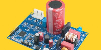
GaN FETs perform for e-bikes, drones and robotics, says EPC

Introducing the EPC9167 GaN-based inverter reference design, Efficient Power Conversion (EPC) said that the FET enhances motor system performance, range, precision and torque, while lowering overall system cost. 

The three-phase brushless DC (BLDC) motor drive inverter uses the EPC2065 eGaN FET. The EPC9167 operates from an input supply voltage between 14 and 60V (nominal 48V) and is available in two configurations – a standard unit and a high current version.

The EPC9167 standard reference design board is a three-phase BLDC motor drive inverter board featuring the EPC2065 eGaN FET rated at 3.6 mOhm maximum RDS(on), 80V maximum device voltage. This standard configuration uses single FETs for each switch position and can deliver up to 20A RMS maximum output current.

For the high current configuration, the EPC9167HC, reference design uses two paralleled FETs per switch position with the ability to deliver up to 42Apk (30A RMS) maximum output current.

Both versions contain all the necessary critical function circuits to support a complete motor drive inverter including gate drivers, regulated auxiliary power rails for housekeeping supplies, voltage, and temperature sense, accurate current sense, and protection functions. The boards feature the ST Microelectronics’ STDRIVEG600, smart motor drive GaN half-bridge driver.

The EPC9167 boards measure just 130 x 100mm (including the connector). The boards can also be configured for multi-phase DC/DC conversion and support both phase and leg shunt current sensing. The boards demonstrate benefits of a GaN-based motor drive, for example lower distortion for lower acoustic noise, lower current ripple for reduced magnetic loss, lower torque ripple for improved precision, and lower filtering for lower cost. 

The EPC9167 boards’ low weight and small size enable them to be integrated into the drive into the motor housing and support low inductance, higher power density motors.

EPC provides full demonstration kits, which include interface boards that connect the inverter board to the controller board development tool for fast prototyping.

The default setting for the GaN-based motor drive kit is 100kHz switching frequency and 14 ns deadtime. The kit is designed to be programmed for different frequencies and deadtimes, although operation at around 100kHz eliminates the need for electrolytic capacitors and allows the use of lower capacitance. It also reduces motor losses, said EPC. The company also advised operating the boards with very small low deadtime of around 14 ns to allow higher torque per Ampere. Combined these features improve inverter and motor system efficiency by more than seven per cent compared with a silicon MOSFET, which typically operates at 20kHz and 500 ns deadtime, said EPC.

The EPC9167 and the EPC9167HC reference design are available for immediate delivery from Digi-Key.

http://www.epc-co.com 

> Read More

0.5Mpixel depth sensor brings 3D depth imaging to mobile devices

The VD55H1 is the first member of a family of high-resolution time-of-flight sensors by STMicroelectronics. According to the company, it brings advanced 3D depth imaging to smartphones and other devices.

The sensor maps three-dimensional surfaces by measuring the distance to over half a million points. Objects can be detected up to 5m from the sensor, and even further with patterned illumination. These parameters mean the VD55H1 addresses emerging AR/VR use cases, including room mapping, gaming and 3D avatars. 

In smartphones, the sensor enhances the performance of camera-system features including Bokeh effect, multi-camera selection and video segmentation. Higher resolution also improves face-authentication security, together with more accurate 3D images to protect phone unlocking, mobile payment and any smart system involving secure transactions and access control. 

The VD55H1 operates with a modulation frequency of 200MHz with more than 85 per cent demodulation contrast at 940nm. This reduces the depth noise by a factor of two over incumbent sensors that typically operate around 100MHz. In addition, multi-frequency operation, a depth-unwrapping algorithm, low pixel noise floor and high pixel dynamic range ensure superior measurement accuracy over long ranging distance, claimed ST. Depth accuracy is better than one per cent and typical precision is 0.1 per cent of distance. 

Other features include a short capture sequence that supports a frame rate up to 120 frames per second and improves motion-blur robustness. Clock and phase management, including spread spectrum clock generator (SSCG), provides multi-device interference mitigation and optimised electromagnetic compatibility (EMC).

The power consumption can be reduced to less than 100mW in some streaming modes, to help prolong the runtime of battery-operated devices, advised ST.

The addition of the VD55H1 3D depth sensor expands the company’s FlightSense products. “The FlightSense portfolio now comprises direct and indirect ToF products from single-point ranging all-in-one sensors to sophisticated high-resolution 3D imagers enabling future generations of intuitive, smart, and autonomous devices,” said Eric Aussedat, ST’s executive vice president, imaging sub-group general manager

VD55H1’s pixel architecture and fabrication process, leveraging in-house 40nm stacked wafer technology, ensures low power consumption, low noise, and optimised die area, confirmed ST. The die contains 75 per cent more pixels than existing VGA sensors, within a smaller die size.

The VD55H1 sensor has a 672 x 804 back-side illuminated (BSI) pixel array for iToF depth sensing. It is now available for lead customers to sample. Volume production maturity is scheduled for the second half of 2022. 

A consumer device form factor reference design for the VD55H1 has been created that includes the illumination system. A supporting fully featured software driver and a library containing an advanced depth-reconstruction image-signal-processing pipeline compatible with Android embedded platforms is also provided. 

http://www.st.com

> Read More

Gen 4 PCIe switches for automotives are first in market, says Microchip

Able to deliver low latency and low power for autonomous driving ecosystems, the Switchtec PFX, PSX and PAX Gen 4 PCIe switches are the first in the market, says Microchip. High speed, low latency connectivity for distributed, heterogenous compute systems are a fundamental element in next-generation autonomous driving applications, said the company. 

The Switchtec PFX, PSX, and PAX switches provide compute interconnect capabilities for advanced driver assistance systems (ADAS). 

“Our automotive-qualified portfolio of Switchtec Gen 4 switches provides the lowest latency and high bandwidth required to link the CPU and accelerator building blocks used in ADAS applications,” said Krishna Mallampati, associate director of marketing and applications for Microchip’s data centre business unit.  

Switchtec Gen 4 PCIe switches provide the high speed interconnect that supports distributed, real time, safety critical data processing in ADAS architectures. As is the case for PCIe’s adoption in the data centre market, it is emerging as the preferred compute interconnect for the automotive industry where it provides low latency and low power bandwidth scalability to CPUs and specialised accelerator devices.

The GPU and computing giant, Nvidia is using the switches in its Drive platform. “The qualification of Microchip’s solutions to meet the stringent needs of the automotive market is a significant milestone, and one Nvidia closely collaborated on,” said Michael Truog, senior director of Automotive Platform Architecture at Nvidia. “Microchip’s automotive PCIe switches deliver flexibility and advanced programmability, enabling high speed SoC and GPU connectivity within our Nvidia Drive platform,” he added. 

The Switchtec automotive-qualified Gen 4 PCIe switches are available in production. Microchip’s ChipLink diagnostic graphical user interface (GUI) provides debug, diagnostics, configuration and forensics tools for rapid deployment.

Microchip Technology provides smart, connected and secure embedded control solutions. development tools and comprehensive product portfolio enable customers to create optimal designs which reduce risk while lowering total system cost and time to market. The company’s products serve customers across the industrial, automotive, consumer, aerospace and defence, communications and computing markets. 

http://www.microchip.com

> Read More

PC-based simulation is blended with 5G network emulator at MWC

Anritsu and dSpace will jointly demonstrate the integration of PC-based simulation systems with sensor-realistic simulation in a 5G network emulator at the Mobile World Congress 2022 (MWC). 

Showcased on the Anritsu stand at the event in Barcelona (28 February to 03 March) the system will demonstrate how to avoid collisions between vehicles and objects or people in intersections with limited visibility. The example application used will be the advanced intersection collision warning (AICW). For this, sensor-based information is exchanged between the vehicles and the infrastructure in the intersection area through the use of 5G communication technology. In the demonstration, V2X data and video data collected by camera sensors is provided and analysed to warn the driver of objects or people (including vulnerable road users) located in blind spots, commonly found at intersections. The demonstration will use 5G network slicing technology to establish a separate URLLC (ultra reliable low latency communications) link to provide V2X hazard warning data and an eMBB (enhanced mobile broadband) link to share high definition (HD) video.

Gregor Hordys, responsible for connectivity topics at dSpace, explained that adding a sensor-realistic and vehicle simulation to the radio communication test system enables testing of advanced applications for connected and co-operative automated driving, based on 5G and edge computing in the lab.

“This joint integration and the power of such a solution is a significant step forward for 5G V2X testing and emulation,” said Jonathan Borrill, Anritsu’s head of global market technology. The demonstration is an example of the development of 5G V2X applications, he added.

To provide a 5G network slicing test environment for automotive V2X use cases, an Anritsu MT8000A radio communication test station and dSpace VEOS (a PC-based simulation platform) will be combined with the dSpace Aurelion for sensor-realistic simulation. 

The Anritsu booth is in Hall 5, D41 at the Mobile World Congress 2022 and at Anritsu’s Virtual MWC22—Wireless Technology Showroom to be launched on February 28. (Registration is required).

http://www.anritsu.com

> Read More

About Smart Cities

This news story is brought to you by smartcitieselectronics.com, the specialist site dedicated to delivering information about what’s new in the Smart City Electronics industry, with daily news updates, new products and industry news. To stay up-to-date, register to receive our weekly newsletters and keep yourself informed on the latest technology news and new products from around the globe. Simply click this link to register here: Smart Cities Registration