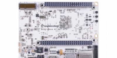
0.5Mpixel depth sensor brings 3D depth imaging to mobile devices

The VD55H1 is the first member of a family of high-resolution time-of-flight sensors by STMicroelectronics. According to the company, it brings advanced 3D depth imaging to smartphones and other devices.

The sensor maps three-dimensional surfaces by measuring the distance to over half a million points. Objects can be detected up to 5m from the sensor, and even further with patterned illumination. These parameters mean the VD55H1 addresses emerging AR/VR use cases, including room mapping, gaming and 3D avatars. 

In smartphones, the sensor enhances the performance of camera-system features including Bokeh effect, multi-camera selection and video segmentation. Higher resolution also improves face-authentication security, together with more accurate 3D images to protect phone unlocking, mobile payment and any smart system involving secure transactions and access control. 

The VD55H1 operates with a modulation frequency of 200MHz with more than 85 per cent demodulation contrast at 940nm. This reduces the depth noise by a factor of two over incumbent sensors that typically operate around 100MHz. In addition, multi-frequency operation, a depth-unwrapping algorithm, low pixel noise floor and high pixel dynamic range ensure superior measurement accuracy over long ranging distance, claimed ST. Depth accuracy is better than one per cent and typical precision is 0.1 per cent of distance. 

Other features include a short capture sequence that supports a frame rate up to 120 frames per second and improves motion-blur robustness. Clock and phase management, including spread spectrum clock generator (SSCG), provides multi-device interference mitigation and optimised electromagnetic compatibility (EMC).

The power consumption can be reduced to less than 100mW in some streaming modes, to help prolong the runtime of battery-operated devices, advised ST.

The addition of the VD55H1 3D depth sensor expands the company’s FlightSense products. “The FlightSense portfolio now comprises direct and indirect ToF products from single-point ranging all-in-one sensors to sophisticated high-resolution 3D imagers enabling future generations of intuitive, smart, and autonomous devices,” said Eric Aussedat, ST’s executive vice president, imaging sub-group general manager

VD55H1’s pixel architecture and fabrication process, leveraging in-house 40nm stacked wafer technology, ensures low power consumption, low noise, and optimised die area, confirmed ST. The die contains 75 per cent more pixels than existing VGA sensors, within a smaller die size.

The VD55H1 sensor has a 672 x 804 back-side illuminated (BSI) pixel array for iToF depth sensing. It is now available for lead customers to sample. Volume production maturity is scheduled for the second half of 2022. 

A consumer device form factor reference design for the VD55H1 has been created that includes the illumination system. A supporting fully featured software driver and a library containing an advanced depth-reconstruction image-signal-processing pipeline compatible with Android embedded platforms is also provided. 

http://www.st.com

> Read More

Gen 4 PCIe switches for automotives are first in market, says Microchip

Able to deliver low latency and low power for autonomous driving ecosystems, the Switchtec PFX, PSX and PAX Gen 4 PCIe switches are the first in the market, says Microchip. High speed, low latency connectivity for distributed, heterogenous compute systems are a fundamental element in next-generation autonomous driving applications, said the company. 

The Switchtec PFX, PSX, and PAX switches provide compute interconnect capabilities for advanced driver assistance systems (ADAS). 

“Our automotive-qualified portfolio of Switchtec Gen 4 switches provides the lowest latency and high bandwidth required to link the CPU and accelerator building blocks used in ADAS applications,” said Krishna Mallampati, associate director of marketing and applications for Microchip’s data centre business unit.  

Switchtec Gen 4 PCIe switches provide the high speed interconnect that supports distributed, real time, safety critical data processing in ADAS architectures. As is the case for PCIe’s adoption in the data centre market, it is emerging as the preferred compute interconnect for the automotive industry where it provides low latency and low power bandwidth scalability to CPUs and specialised accelerator devices.

The GPU and computing giant, Nvidia is using the switches in its Drive platform. “The qualification of Microchip’s solutions to meet the stringent needs of the automotive market is a significant milestone, and one Nvidia closely collaborated on,” said Michael Truog, senior director of Automotive Platform Architecture at Nvidia. “Microchip’s automotive PCIe switches deliver flexibility and advanced programmability, enabling high speed SoC and GPU connectivity within our Nvidia Drive platform,” he added. 

The Switchtec automotive-qualified Gen 4 PCIe switches are available in production. Microchip’s ChipLink diagnostic graphical user interface (GUI) provides debug, diagnostics, configuration and forensics tools for rapid deployment.

Microchip Technology provides smart, connected and secure embedded control solutions. development tools and comprehensive product portfolio enable customers to create optimal designs which reduce risk while lowering total system cost and time to market. The company’s products serve customers across the industrial, automotive, consumer, aerospace and defence, communications and computing markets. 

http://www.microchip.com

> Read More

PC-based simulation is blended with 5G network emulator at MWC

Anritsu and dSpace will jointly demonstrate the integration of PC-based simulation systems with sensor-realistic simulation in a 5G network emulator at the Mobile World Congress 2022 (MWC). 

Showcased on the Anritsu stand at the event in Barcelona (28 February to 03 March) the system will demonstrate how to avoid collisions between vehicles and objects or people in intersections with limited visibility. The example application used will be the advanced intersection collision warning (AICW). For this, sensor-based information is exchanged between the vehicles and the infrastructure in the intersection area through the use of 5G communication technology. In the demonstration, V2X data and video data collected by camera sensors is provided and analysed to warn the driver of objects or people (including vulnerable road users) located in blind spots, commonly found at intersections. The demonstration will use 5G network slicing technology to establish a separate URLLC (ultra reliable low latency communications) link to provide V2X hazard warning data and an eMBB (enhanced mobile broadband) link to share high definition (HD) video.

Gregor Hordys, responsible for connectivity topics at dSpace, explained that adding a sensor-realistic and vehicle simulation to the radio communication test system enables testing of advanced applications for connected and co-operative automated driving, based on 5G and edge computing in the lab.

“This joint integration and the power of such a solution is a significant step forward for 5G V2X testing and emulation,” said Jonathan Borrill, Anritsu’s head of global market technology. The demonstration is an example of the development of 5G V2X applications, he added.

To provide a 5G network slicing test environment for automotive V2X use cases, an Anritsu MT8000A radio communication test station and dSpace VEOS (a PC-based simulation platform) will be combined with the dSpace Aurelion for sensor-realistic simulation. 

The Anritsu booth is in Hall 5, D41 at the Mobile World Congress 2022 and at Anritsu’s Virtual MWC22—Wireless Technology Showroom to be launched on February 28. (Registration is required).

http://www.anritsu.com

> Read More

Server increases node density for 5G, IoT and edge applications

Short depth, multi-node servers have been designed and optimised by Supermicro for 5G, IoT, and edge applications. The SuperEdge server is suitable for environments where high-density compute and I/O are required in a small form factor, for example, on-site in retail or branch offices, or field locations such as at the base of cell towers or high traffic areas. 

The SuperEdge uses a third generation Intel Xeon Scalable processor in each node to deliver data centre processing power at the edge to accelerate analysis and real-time application functionality. The server increases node density by 50 per cent over previous application-optimised servers for 5G, IoT, and Edge workloads, said Supermicro. Customers can start with a single server and add additional ones as demand increases.

“The SuperEdge server increases the compute and I/O densities for edge applications and enables operators to increase system workloads and data processing performed at the edge, reducing network traffic back to data centres,” said Charles Liang, president, and CEO, Supermicro. “Designing application-tuned servers for both the edge and the cloud optimises the deployment of network computing, as we move to the metaverse,” he added.

The Supermicro SuperEdge server is designed to fit in small data centres or environments where server depth is critical. It has a depth of just 430mm and GPUs (graphics processing units) may also be installed, giving the Supermicro SuperEdge the ability to perform AI calculations at the edge of the network, increasing decision-making capabilities and reducing response times.

The nodes and I/O connections are accessible from the front, allowing quick maintenance when needed. The server will operate across a temperature range of -5 to +55 degrees C and is suitable for a range of humidity and other environmental conditions. It can therefore be installed where there is no climate controlled setting without increasing opex (operating expenditure). Redundant power supplies and cooling fans enable the SuperEdge server to operate in harsh conditions outside of a traditional data centre.

Each of the three hot-swappable nodes can accommodate three PCIe 4.0 slots, which enable a range of add-on cards that accelerate applications designed for edge computing. The server’s I/O density allows for multiple acceleration cards, including networking, FPGA, DPU, eASIC and TimeSync options. Each node can accommodate up to 2Tbyte of DDR4 DRAM. This allows more extensive and more complex applications to be installed and executed than previously available, added the company.

http://www.supermicro.com

> Read More

About Smart Cities

This news story is brought to you by smartcitieselectronics.com, the specialist site dedicated to delivering information about what’s new in the Smart City Electronics industry, with daily news updates, new products and industry news. To stay up-to-date, register to receive our weekly newsletters and keep yourself informed on the latest technology news and new products from around the globe. Simply click this link to register here: Smart Cities Registration