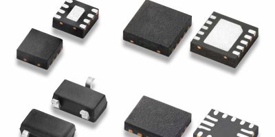
Program partners FPGA-based IP with Bittware accelerator technologies 

Pairing new FPGA-based IP from partner companies with BittWare’s compute, network, storage and sensor processing accelerator products, the BittWare Partner Program intends to reduce risk while accelerating time to market. 

As FPGAs increase in size, complexity and performance, the development of customized IP and board level capabilities can prove time-consuming, expensive and resource-intensive. The BittWare Partner Program is designed to simplify and streamline customer deployments of these high performance, data intensive applications.  According to BittWare it removes major time-to-market and technology hurdles by facilitating an ecosystem of FPGA-based enablement IP and full solutions that use BittWare’s proven FPGA accelerator technology.

The programme empowers FPGA designers to access a robust ecosystem of proven IP cores, tools, frameworks and solutions from a central source, explains Craig Petrie, vice president of sales and marketing at BittWare. “In doing so, we are uniquely positioned to close critical gaps in the FPGA design process while reducing risk and accelerating commercialisation of innovative, high-performance applications.”

The partner programme aligns products from industry-leading and emerging IP providers with BittWare’s compute, network, storage and sensor processing accelerator technologies. In addition to achieving faster out-of-the-box functionality, the ability to combine critical components of the FPGA design process reduces engineering and programming requirements, points out the company. This enables customers to focus in-demand resources on developing other capabilities.

Customers have the opportunity to collaborate much earlier in the design process to meet the varying demands of powerful next-generation applications, such as AI, machine learning inference, database acceleration, computational storage, 5G, test and measurement and security.

The inaugural list of ten partners includes Intel – BittWare leverages the Intel Agilex FPGA technology and oneAPI toolkits to simplify development of high performance computing (HPC) applications; EdgeCortix (an edge AI-focused fabless semiconductor company) and Megh Computing, provider of real-time, AI-based video analytics. For network development, Atomic Rules provides mission-critical, enterprise-grade IP cores and solutions from the data centre to the edge; Enyx specialises in low latency, FPGA-enabled technologies for the financial, telecomms and HPC sectors; Grovf develops application acceleration and network offload solutions using FPGA chips; Siama Systems specialises in Ethernet/IP network infrastructure test for 5G RAN, MEC and data centres and Xiphera develops cryptographic IP cores, designed directly for FPGAs.

Other partners address storage, namely Eideticom (computational storage for cloud, HPC and enterprise data centres) and IntelliProp, which provides IP cores, ASIC design and verification services for the storage industry.
BittWare, a Molex company, designs and manufactures enterprise-class FPGA hardware.

Molex has a presence in more than 40 countries, and enables technology innovation in the automotive, data centre, industrial automation, healthcare, 5G, cloud and consumer device industries. 

http://www.molex.com.

> Read More

Tasking extends the VX-toolset for Arm with Traveo T2G support

Version 6.0r1 of the VX-Toolset compiler toolchain for Arm Cortex-M also supports Infineon’s Traveo T2G microcontroller family. 

The Traveo T2G microcontroller family is based on Arm’s Cortex-M4 / Cortex-M7. Infineon and Tasking have worked on software development tools for TriCore/Aurix (TC2x, TC3x and TC4x) and now with support for the Traveo T2G family, Tasking offers toolchains for Infineon’s entire microcontroller portfolio. Having compilers for both Traveo T2G and Aurix available from a single tool partner simplifies the work of users who use both microcontrollers. 

The VX-Toolset for Arm Cortex-M is qualified according to ISO 26262 up to ASIL D. TÜV certification is planned for this year. 

Tasking supplies a safety manual with the toolchain. As long as users follow the recommendations described there, they can use the toolchain for the development of safety-critical applications up to ASIL D without any further qualification measures, advises the company. This significantly simplifies and accelerates the certification of the system and reduces costs for the customer, says Tasking.

The VX-toolset for Arm Cortex-M v6.0r1 is available immediately. 

Tasking Germany specialises in providing embedded software development tools. The company is headquartered in Munich, Germany. Tasking development tools are used by automotive manufacturers and the world’s largest Tier 1 supplier to realise high-performance applications in safety critical areas. The tools are used to develop the latest applications to optimum reliability, functional safety and performance standards.

http://www.tasking.com

> Read More

Clock buffers and multiplexers meet PCIe Gen6 specifications

Believed to be the first clock buffers and multiplexers on the market to meet stringent PCIe Gen6 specifications, the RC190xx clock buffers and RC192xx multiplexers have been released by Renesas. 

The release comprises 11 clock buffers and four multiplexers. The devices, which also support and provide extra margin for PCIe Gen5 implementations, complement Renesas’ low-jitter 9SQ440, 9FGV1002 and 9FGV1006 clock generators for PCIe Gen6 timing for data centre / cloud computing, networking and high-speed industrial applications.

The PCIe Gen6 standard supports extremely high data rates of 64Gtransfers per second while requiring very low clock jitter performance of less than 100fs RMS. The RC190xx clock buffers and RC192xx multiplexers have PCIe Gen6 additive jitter specs of only 4fs RMS, making them virtually noiseless, says Renesas. The company claims this means they future-proof designs for the next generation of industry standards.

“PCIe Gen6 timing will be at the heart of new equipment in data centers, high-speed networking and other applications,” said Zaher Baidas, vice president of the Timing Products division at Renesas. 

“It will be interesting to see the innovative implementations that result from this new capability, especially when considering how solutions for the emerging Chiplet market are starting to evolve, with the need for increasing speed and bandwidth as an underlying constant,” comments Rich Wawrzyniak, principal analyst for Semico Research.

The PCIe Gen6 clock buffers and multiplexers offer 1.4ns in-out delay, 35ps out-out skew and -80dB PSRR (power supply rejection ratio) at 100kHz in addition to low 4fs PCIe Gen6 additive jitter. 

Selectable SMBus addresses facilitate the use of multiple devices while SMBus write-protect feature enhances system security. 

The devices represent 30 per cent space-saving compared to earlier devices, adds Renesas.

Other features are loss-of-signal (LOS) output supports system monitoring and redundancy, a four-wire side-band interface to support high speed serial output enable / disable and device daisy-chaining. In addition, power down tolerant (PDT) and flexible start-up sequencing (FSS) features ensure good behaviour under abnormal system conditions, the company claims.

The RC190xx buffers are offered in 4-, 8-, 13-, 16-, 20- and 24-output configurations. The RC192xx multiplexers include 2-, 4-, 8- and 16-output versions. They are offered in packages as small as 3.0 x 3.0mm. 

All of the new devices are available now, and Renesas also offers an evaluation board schematic. 

http://www.renesas.com

> Read More

Wideband transceiver test reveals RF characteristics of mixed digital devices

To accelerate the design cycle, Keysight Technologies has introduced a digital wideband transceiver test system, which it claims unveils true radio frequency (RF) performance characteristics of mixed-digital RF devices.

Defense radars and satellite communications and 5G employ phased-array antennas (PAA) to meet performance and versatility requirements to millimeter wave frequencies. Digital signals are highly integrated into the RF front-end architecture of modern antennas used in defence radar, satellite communications and 5G. As a result, the antennas need a new measurement methodology for stimulus and response measurements, says Keysight.

Its digital wideband transceiver test comprises a vector network analyser, device measurement software and transceiver analysis software to compare digital and RF signals between device input and output and measures the transmitter and receiver responses independently from other test instrumentation. 

The test system uses Keysight’s N52xxB PNA/PNA-X vector network analyser. This is an integrated, flexible microwave test engine for measuring active devices, such as amplifiers, mixers and frequency converters. It also includes S94601B device measurement eXpert software, a configuration assistant that enables users to set up complex measurements for various types of devices. There is also S94610B digital wideband transceiver analysis software. This test waveform creator and configuration assistant enables users to set up mixed-digital RF devices.

Wideband stimulus waveforms are generated by Keysight’s VXG vector signal generator (M938xB) and the PNA-X device measurement eXpert software enables device characterisation and a control interface. The RF test equipment’s measurement and signal fidelity tests new mixed-digital RF devices, and is claimed to minimising errors to yield highest possible performance characteristics.

According to Dan Dunn, vice president of Keysight’s Aerospace & Defense Government Solutions: “Keysight’s digital wideband transceiver test solution enables true RF performance characterisation, while speeding measurements and data analysis that ultimately accelerate the entire design cycle.”

Keysight says the digital wideband transceiver test solution reduces weeks of in-house measurement and data analysis effort to a few minutes. It can be leveraged to component level, such as ADCs, DACs and transceiver ICs as well as sub-system level such as radar / electronic warfare transmit and receive modules, satellite communications transmitters / receivers. For system level, it addresses whole signal paths of 5G PAAs (phased array antennas) using massive multiple-input, multiple-output (MIMO) technology.

The system maintains high measurement accuracy of GHz bandwidth in mm wave frequencies and adapts to proprietary digital designs.

http://www.keysight.com

> Read More

About Smart Cities

This news story is brought to you by smartcitieselectronics.com, the specialist site dedicated to delivering information about what’s new in the Smart City Electronics industry, with daily news updates, new products and industry news. To stay up-to-date, register to receive our weekly newsletters and keep yourself informed on the latest technology news and new products from around the globe. Simply click this link to register here: Smart Cities Registration