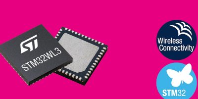
Integrated, low power, single-chip LCOS panel fits into AR/XR/MR glasses

The OP03011 liquid crystal on silicon (LCoS) panel integrates the array and frame buffer into an ultra-compact single-chip solution that is lightweight and low-power for smart glasses

The OP03011 is a single chip, 648p LCoS panel for next generation augmented reality (AR), extended reality (XR) and mixed reality (MR) glasses and head-mounted displays. The LCOS panel features 3.8 micron pixels in what is claimed to be one of the world’s smallest 0.14-inch optical formats. The low power, lightweight design is intended for next-generation glasses that can be worn 24/7, said Omnivision.

The growing interest in AR glasses has led OEMs to design more functionality into slim, fashionable designs that consume very little power and are lightweight, allowing them to be worn for long periods. The OP03011 is designed in a compact format for applications requiring a smaller field of view and lower resolution, making it well suited for some of the sleekest, most innovatively designed AR glasses, said Devang Patel, marketing director for the IoT and emerging segment, Omnivision. “The OP03011 supports applications of next-generation smart glasses, like displaying notifications in the user’s field of view and access to GPS for maps and directions directly from the glasses, so the user never needs to pull out their smartphone,” he said.

The OP03011 features 648 x 648 resolution at 120Hz and comes in a small FPCA package. It supports a single-lane MIPI-DSI interface. 

Samples are available now, and the OP03011 will be in mass production in Q4 of 2023.

Omnivision is a fabless semiconductor company that develops advanced digital imaging, analogue and touch and display solutions for multiple applications and industries, including mobile phones, security and surveillance, automotive, computing, medical, and emerging applications. 

http://www.ovt.com

> Read More

Cadence introduces tools for Arm TCS23 for a fast path to tapeout

Cadence has finetuned its RTL-to-GDS digital flow and delivered corresponding 3nm and 5nm rapid adoption kits (RAKs) for Arm Cortex-X4, Cortex-A720 and Cortex-A520 CPUs and Immortalis-G720, Mali-G720 and Mali-G620 GPUs.

This part of Cadence Design Systems’ expanding collaboration with Arm to advance mobile device silicon, providing customers with a faster path to tapeout through the use of Cadence digital and verification tools and the new Arm Total Compute Solutions 2023 (TCS23) for the cores and GPUs.

Cadence delivered comprehensive RTL-to-GDS digital flow RAKs for 3nm and 5nm nodes to help customers achieve power and performance goals using the new Arm TCS23. The Cadence tools optimised for the new Arm TCS23 include the Cadence Cerebrus Intelligent Chip Explorer, Genus Synthesis, Modus DFT software, Innovus implementation system, Quantus extraction, Tempus timing signoff and ECO Option, Voltus IC Power Integrity, conformal equivalence checking and conformal low power. Cadence Cerebrus provided Arm with AI-driven design optimisation capabilities that resulted in 50 per cent better timing, a 10 per cent reduction in cell area and 27 per cent improved leakage power on the Cortex-X4 CPU, empowering Arm to achieve power, performance and area (PPA) targets faster, reported Cadence.

The digital RAKs provide Arm TCS23 users with benefits, for example the AI-driven Cadence Cerebrus automates and scales digital chip design, providing customers with improved productivity versus a manual, iterative approach. Cadence iSpatial technology provides an integrated implementation flow, offering improved predictability and PPA, leading to faster design closure. The RAKs also incorporate a smart hierarchy flow that enables accelerated turnaround times on large, high-performance CPUs. The Tempus ECO Option, which provides path-based analysis, is integrated into the flow for signoff-accurate, final design closure. Finally, the RAKs use the GigaOpt activity-aware power optimisation engine, incorporated with the Innovus implementation system and the Genus Synthesis to dramatically reduce dynamic power consumption.

Arm used the Cadence verification flow to validate the Cortex-X4, Cortex-A720 and Cortex-A520 CPU-based and Immortalis-G720, Mali-G720 and Mali-G620 GPU-based mobile reference platforms. The Cadence verification flow supports Arm TCS23 and includes the Cadence Xcelium logic simulation platform, Palladium Z1 and Z2 Enterprise emulation platforms, Helium Virtual and Hybrid Studio, JasperÒ formal verification platform and Verisium Manager planning and coverage closure tools.

The Cadence verification flow lets Arm TCS23 users improve overall verification throughput and leverage advanced software debug capabilities. Cadence also validated that Cadence Perspec system verifier, VIP and System VIP tools all support TCS23-based designs to enable customers to accelerate time to market when assembling TCS23-based SoCs. The virtual and hybrid platform reference designs include the Arm Fast Models to enable early software development and verification through the Cadence Helium Studio as well as the Cadence Palladium and Protium platforms, also known as the dynamic duo.

The Cadence digital and verification flows support the Cadence Intelligent System Design strategy, which enables customers to achieve SoC design excellence. 

http://www.cadence.com 

> Read More

Renesas adds three motor control MCU groups drawn from multiple families

Targeting motor control applications, Renesas Electronics has introduced three microcontroller (MCU) groups, including devices from its RX and RA families.

There are two new MCU groups from the RA family of Arm Cortex-M devices. The RA4T1 Group delivers 100MHz performance with up to 256kbyte of flash and 40kbyte SRAM. The MCUs are based around 100MHz Arm Cortex-M33 CPU cores with TrustZone and have integrated flash memory options from 128kbyte to 256kbyte and 40kbyte SRAM. In addition to an integrated trigonometric function unit as a hardware accelerator, they feature integrated analogue functions, including 12bit ADC, PGA, comparator and 12bit DAC. The MCUs are available in 32- to 64-pin packages options.

The second addition is the RA6T3 Group which offers 200MHz operating frequency and provides 256kbyte of flash and 40kbyte SRAM. These are based around a 200MHz Arm Cortex-M33 CPU core with TrustZone and have integrated flash memory of 256kbyte and 40kbyte SRAM.  They have the same analogue functions as the RA4T1 Group and integrated communications options including USB 2.0, CAN FD, I3C, SCI and SPI. They are available in package options from 32- to 64-pin.

Both new groups offer features and functions specifically for motor control applications, including trigonometric function units (TFUs) for acceleration, advanced ADC with integrated PGA (programmable gain amplifier), with a choice of communication interfaces including CAN FD. 

The MCUs are supported by the Renesas Flexible Software Package (FSP) to allow designers to port designs from other RA family devices.

Another introduction is the RX26T Group of MCUs from the RX family operating at 120MHz with up to 512kbyte of flash memory and 64kbyte SRAM. Renesas claimed that it has industry-leading real-time performance of 120MHz with no-wait flash memory access. The MCUs support 5.0V power supplies with high noise immunity and control accuracy, added Renesas. They also provide TFUs, on-chip timing, and interrupt control. Designers using Renesas’ RX24T MCUs can scale designs to the RX26T devices to take advantage of existing design software while realising performance and control efficiency improvements, said Renesas. 

All of the new MCUs are available now and supported by Renesas’ Flexible Motor Control development kit that enables easy evaluation of motor control using permanent magnet synchronous motors (brushless DC motors), and the Renesas Motor Workbench development tool.

http://www.renesas.com 

> Read More

Secure i.MX 91 processors bring Linux to the edge, says NXP

Bringing Linux capabilities to “thousands of edge applications” the i.MX 9 series of processors streamlines the development of cost-optimised edge devices that require security, performance and Linux support in a scalable, reliable platform, said NXP Semiconductors.

The processors are designed for the next generation of Linux-based IoT and industrial applications.

Emerging protocols, such as Matter or the ISO 15118-20 standard for electric vehicle (EV) chargers, create inflection points for new products, many of which rely on Linux for use in IoT and industrial markets. The i.MX 91 family has been developed to enable users to quickly create new Linux-based edge devices, such as home controllers, connected appliances, home entertainment, industrial scanning and printing, building control, EV chargers and medical platforms, advised NXP.

The i.MX 91 is the entry point of the i.MX 9 series and has hardware and software commonality with NXP’s i.MX 93 family. 

It will “provide the foundation for thousands of new device classes, with its high performance, connectivity and EdgeLock secure enclave setting a new standard for Linux platforms across IoT and industrial applications,” said Charles Dachs, senior vice president and general manager, of industrial and IoT edge, at NXP. He continued: “The i.MX 91 family enables the rapid development of platforms that may easily pivot into new markets and new applications, leveraging existing investments and streamlining product line updates.”

The i.MX 91 applications processor features an Arm Cortex-A55 running at up to 1.4GHz with support for LPDDR4 memory and dual Gigabit Ethernet for gateway or multi-network segment support. There are also dual USB ports and I/O for products in smart factory, smart home, smart office, medical device, metering and cost-optimised system on module platforms.

An integrated EdgeLock secure enclave provides lifecycle management, tamper detection, secure boot, and a simplified path to certifications. These important security capabilities are easily accessed by the developers through NXP-provided security software enablement.

The i.MX 91 family is available with NXP’s co-developed and cost-optimised power management solution, available as part of the i.MX 93 family ecosystem. The evaluation kits and software packages for the i.MX 91 family integrate with NXP’s scalable wireless portfolio which includes the IW612, the industry’s first monolithic tri-radio family that supports Wi-Fi 6, Bluetooth 5.2 and 802.15.4. The IW612, focused on Matter, frees consumers from the restrictions of single-protocol ecosystems, allowing them to enjoy seamless interoperability across different ecosystems and wireless network technologies.

NXP’s i.MX applications processors are available worldwide through distributors and eTailers. They are enabled by NXP software, a broad ecosystem of tools and software, and comprehensive support. To help ensure a stable supply of products for embedded designs, all i.MX 8 series and i.MX 9 series products are guaranteed for a minimum of 15 years of availability as members of the NXP product longevity programme.

NXP expects to enable select customers with i.MX 91 development platforms in the second half of 2023 as part of the early access programme. 

http://www.nxp.com

> Read More

About Smart Cities

This news story is brought to you by smartcitieselectronics.com, the specialist site dedicated to delivering information about what’s new in the Smart City Electronics industry, with daily news updates, new products and industry news. To stay up-to-date, register to receive our weekly newsletters and keep yourself informed on the latest technology news and new products from around the globe. Simply click this link to register here: Smart Cities Registration