Panasonic Industry has launched a new member of its Grid-EYE sensor family featuring a 90° lens delivering a wider field of view (FoV) and reducing the number of sensors required to cover a given area to enable people counting and tracking applications. Privacy conscious designers have appreciated the 64 pixel resolution of the Grid- EYE family, and the Grid- EYE 90° will enhance systems designed to track and count the movement of people tracking as well as other applications.
Comments Osamu Mitsumura, Product Manager at Panasonic Industry Europe: “Knowing where people are is the key to design a smart space. Today, industries want to understand and optimise how their buildings are being used, especially the businesses in retail, hospitality and healthcare. Similarly, the lighting industry is increasingly moving towards providing personalised ambient spaces. The pandemic has also highlighted the importance of management of highly frequented or confined spaces – like offices or public washroom facilities. The holy grail of people-tracking/counting solutions has always been Scalability and cost-effectiveness. Grid-EYE 90° delivers both.”
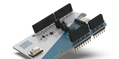
A new sensor with 90° field of view for privacy conscious people tracking
Previously, Grid-EYE has been used in a variety of applications where absolute temperature values are used for detecting hot spots in a smart kitchen or hotter areas of a room for smart air conditioning.
At the same time, Grid-EYE is also highly suitable for people tracking/counting applications. Innovative product designers have used Grid-EYE 60° as a cost-effective alternative to camera or wireless solutions.
The new variant of Grid-EYE builds on Panasonic’s deep expertise of innovative sensing technologies. The new 90° wide-angle lens allows Grid-EYE to have a wider field of view (FoV), improving on previous sensors which offer a 36° and 60° FoV. With the launch of Grid-EYE 90°, system designers can capture the IR signature of a larger area, so fewer sensors are required to cover a given area. This makes it an ideal choice for enhancing the efficiency of people tracking/counting devices.
Successful data acquisition using Grid-EYE is only the first step in successfully counting people. Different techniques can be employed to exploit the sensor data. The use of standard signal processing algorithms works well, but can run into difficulties with infrared sensors. Unlike visual spectrum devices where the quality of data is unambiguous, infrared signals can be tricky to handle when employed in devices – especially the ones with low resolution which can pick up noise very easily, such as Grid-EYE. Everyday occurrences like a hot coffee cup, an open window or an overheating computer, which are not even a subject of discussion in the visual spectrum, are daunting challenges in infra-red. This makes the algorithm development much more complex.
One way to overcome this problem is to use machine learning (ML). ML is a subset of Artificial Intelligence (AI) techniques, that emphasises on the use of self-learning neural networks to derive inferences from the input data. The neural network can be trained using a known annotated dataset to design a ML model, which can be then deployed in field. This allows offloading complex tasks to neural networks, which previously required customised algorithm and expensive hardware.
An ML model with good performance can only be built by training on a good quality dataset. Contrary to more common applications like computer vision where there are rich datasets already available, sensors like Grid-EYE do not often have any datasets to begin with. Recognising the need to bridge this gap, Panasonic has started a collaboration with CN Group, a software company which is part of the Ciklum company. CN Group has expertise in a wide array of topics including mechanical design, embedded electronics hardware and software, machine learning and IoT. Using a hardware setup which includes Grid-EYE sensor and a camera, CN Group is working to build datasets containing visual and thermal information from an observed scene. Furthermore, using computer vision techniques, the dataset is automatically annotated when humans are detected in the field of view of the camera. CN Group’s contribution in creating quick annotated datasets opens a wide array of possibilities in creating customised thermal datasets for any given location – meeting rooms, staircases, etc. Panasonic and CN group believe that that this collaboration will enable more customised/personalised ML systems for people-tracking/counting using Grid-EYE.
Learn more on the sensor on Panasonic Industry’s website http://industry.panasonic.eu